Self-texturizing electronic properties of a 2-dimensional GdAu2 layer on Au(111): the role of out-of-plane atomic displacement
We demonstrate the spontaneous patterning of the electronic properties of a 2-dimensional layer
One of the major issues of nanoscience and the promotion of technological applications is the formation of layers whose electronic and chemical properties are patterned at nanoscale. The research team composed by investigators of the University of the Basque Country and of the CNR-IOM-Trieste has demonstrated that the electronic properties of a weakly interacting 2-dimensional layer at nanoscale spontaneously texturize. The fundamental factors leading to the spatial modulation of the electronic properties are the structural relaxation processes and the variable adsorption stacking configurations. We believe that these provide an easy and elegant @method to template the electronic structure of interfaces characterized by a variable atomic stacking registry commonly observed in mismatched 2-dimensional layers leading to Moiré superstructures. Notwithstanding that these Moiré superstructures are quite commonly observed at the interface of 2D-materials, little attention has been paid on the buckling-induced patterning of their electronic properties. In this work we have demonstrated that the departure of the 2D layer from the perfect crystallographic flatness, typical of graphene, satisfies the expectation and allows tuning the electronic properties of two-dimensional (2D) layers.
A bi-metallic monolayer alloy demonstrated the spontaneous patterning of the electronic properties upon the formation of the interface
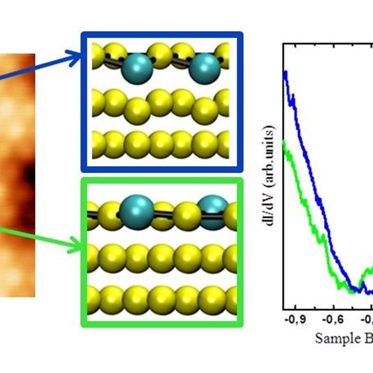
Specifically, we have characterized a bi-metallic monolayer alloy, namely GdAu2, obtained upon evaporation of gadolinium atoms on the annealed Au(111) surface, which results in a weakly interacting Moiré superstructure and demonstrated the spontaneous patterning of the electronic properties upon the formation of the interface. We have shown that the variable adsorption stacking configuration induces a layer-buckling at the mismatch GdAu2/Au(111) interface. The layer/substrate coupling, and the induced out-of-plane displacement of the Gd atoms is sufficient to locally open an energy gap of ∼0.5 eV at the Fermi level in an otherwise metallic layer, and to pattern the character of the hybridized Gd-d states. These and the observed shift of the center of mass of the Gd 4f multiplet, proportional to the lattice distortion, demonstrate the close correlation between the electronic properties of the 2D-layer and its planarity. We demonstrate that the resulting template shows different chemical reactivity which may find important applications.
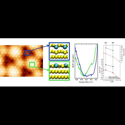
GdAu2/Au(111) moire pattern, local structural relaxation and modulation of the electronic properties from the Fermi level to the Gd4f states
NFFA-EUROPE FACILITIES AND TECHNIQUES
XPS and IPES inverse photoemission techniques (@ CNR-IOM )
DFT-Calculation ( @ CNR-Democritos)
PUBLICATION DETAILS
September 28th, 2017 - nanoscale, 2017,9, 17342-17348
Self-texturizing electronic properties of a 2-dimensional GdAu2 layer on Au(111): the role of out-of-plane atomic displacement
Alexander Correa a,b,c, Matteo Farnesi Camellone d, Ana Barragan a,c, Abhishek Kumar e,f, Cinzia Cepek e, Maddalena Pedio e , Stefano Fabris d Lucia Vitali a,c,g
a Departamento de Física de Materiales, Universidad del País Vasco, ES-20018 San Sebastián, Spain. b Donostia International Physics Center, ES-20018 San Sebastián, Spain. c Centro de Fisica de Materiales (CSIC-UPV/EHU) y Material Physics Center, ES- 20018 San Sebastián, Spain. d CNR-IOM DEMOCRITOS, Istituto Officina dei Materiali, Consiglio Nazionale delle Ricerche and SISSA, I-34136 Trieste, Italy. e Istituto Officina Materiali (CNR-IOM), Laboratorio TASC, I-34149 Trieste, Italy. f Dipartimento di Fisica, Università di Trieste, I-34127 Trieste, Italy. g Ikerbasque Foundation for Science, ES-48013 Bilbao, Spain
Reference: DOI: 10.1039/C7NR04699E | nanoscale, 2017,9, 17342-17348
For more information: Dr. Lucia Vitali, lucia.vitali@ehu.es; Dr. Stefano Fabris, fabris@democritos.it

