Current conduction mechanism and electrical break-down in InN grown on GaN

HERAKLION, GREECE- BRATISLAVA, SLOVAKIA.Future ultra-high-frequency transistors may be designed with InN channel material. In fact, this approach may lead to the fastest solid-state transistors ever due to the extremely high theoretical electron velocity of InN. However, electron velocity in InN channel transistors has never been measured.
(GaN)/InN samples were grown in a Molecular-Beam Epitaxy (MBE) system equipped with nitrogen RF plasma source. A careful preparation of the growth chamber/vacuum and the source materials was employed to limit the incorporation of unintentional donor impurities, such as oxygen atoms, in the InN layers. GaN buffer was MBE grown on a commercially available high-resistivity GaN-on-sapphire template, followed by an InN film. An optimized InN growth process was carried out, according to the results of our previous InN MBE investigations.
the study confirmed feasibility of InN channel transistors, reaching electron velocity far above conventional GaN
The InN films were initially characterized by conductivity and Hall Effect measurements ranging from room temperature (RT) down to 20 K, by high-resolution X-ray diffraction (HRXRD), and by photoluminescence (PL).
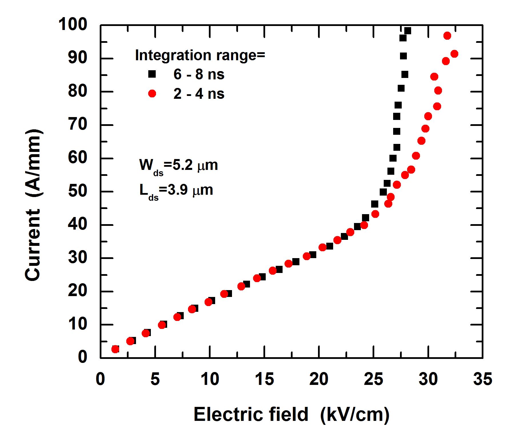
Special test structures have been used to characterize InN resistors using current-voltage short pulses. Premature breakdown has appeared before reaching current/velocity saturation, which was linked to defects in InN due to heteroepitaxial growth and strain relaxation. As pointed by Georgakilas, InN growth needs further advancement. Nevertheless as said by Kuzmik, our study confirmed feasibility of InN channel transistors, reaching electron velocity far above conventional GaN.
Applied Phys. Lett. 110 (2017) 232103
Current conduction mechanism and electrical break-down in InN grown on GaN
J. Kuzmik, C. Fleury, A. Adikimenakis, D. Gregušová, M. Ťapajna, E. Dobročka, Š. Haščík, M. Kučera, R. Kúdela, M. Androulidaki, D. Pogany, and A. Georgakilas
Reference: https://doi.org/10.1063/1.4985128
The Institute of Electronic Structure and Laser (IESL) of the Foundation for Research and Technology Hellas has a unique complete III-V microelectronics facility in Greece jointly with the Physics Department of University of Crete.
Facilities, directly related to this project, include: (1) an MBE growth laboratory installed in a class-1000 clean room, having a RIBER 32P MBE system with nitrogen RF-plasma source for growth of III-Nitrides, (2) a complete device fabrication laboratory installed in a class-1000 clean room, with deep-UV mask aligner with backside alignment capability, e-beam evaporator, RF and DC sputtering, RIE and PECVD systems and (3) a full line of optical, electrical and structural material and device characterization techniques, such as 14-300K PL, micro-PL, PR, ER, C-V, DLTS, quasistatic I-V, RF S-parameter, noise and power measurements up to 20 GHz, on-wafer RF probes, AFM, SEM, Nomarski, HRXRD.
Jan Kuzmik Jan.Kuzmik@savba.sk
Institute of Electrical Engineering - Slovak Academy of Sciences
Dubravska cesta 9
841 04 Bratislava
Slovakia

