Direct-write method to grow individual and 3D superconducting hollow nanowires

ZARAGOZA, SPAIN - Superconductors are commonly utilized in several applications such as energy generators and storage due to their unique capability of transferring electricity without energy losses. Miniaturization in superconductors can optimize their functionality and, furthermore, when the miniaturization reaches the nanoscale, in the range of the superconducting coherence length, novel physical phenomena can arise.
On the other hand, 3D superconductors are expected to promote a change in the development of the next generation of electronic devices. Nevertheless, their fabrication is still challenging and only a few articles addressing the growth of 3D have been reported yet.
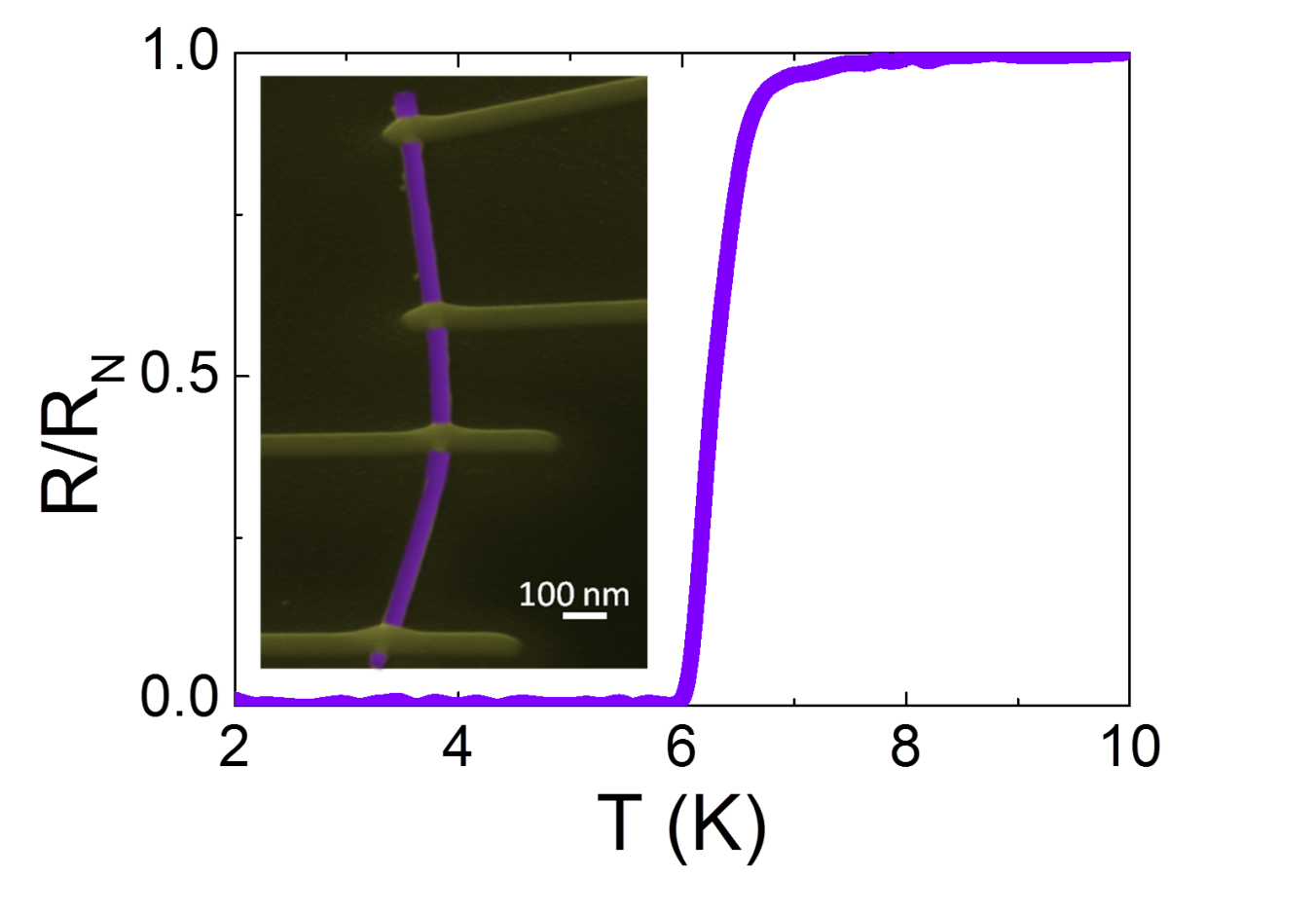
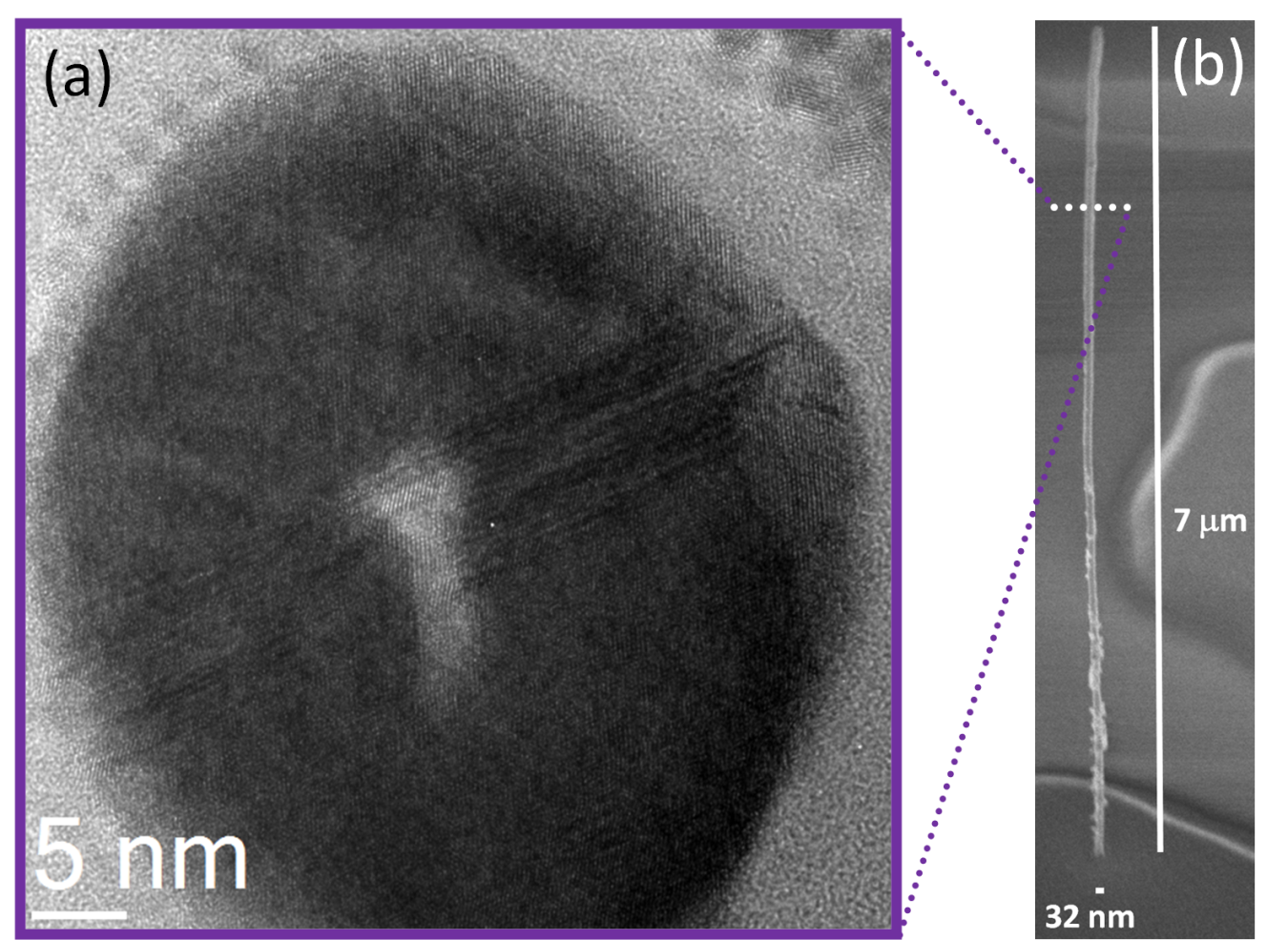
"Our work is the first to successfully fabricate and characterize 3D superconducting crystalline WC hollow nanowires with diameters down to 32 nm and aspect ratio above 200 ".
The method is based on using highly-focused beam of He+ ions to decompose a W(CO)6 precursor. The growth of the vertical WC nanowire occurs around the ion beam spot, mainly due to the interaction of secondary electrons with the adsorbed precursor molecules, whereas a cavity at the center of the nanowire is created due to the He+ beam milling effect on the growing material. The small nanowire diameter achieved is due to the use of a very small He+ beam spot (<1 nm).
"Without the training I followed in the handling of the He+ microscope carried out by Prof. Dominique Mailly, the facility scientist, the fabrication of high quality vertical WC hollow nanowires would have not been possible".
The nanowires exhibit 1.5 times higher superconducting critical temperatures (6.4 K) as well as 1.5 times higher upper critical magnetic fields (≈14 T) when compared to nanowires grown by Ga+ FIBID.
"This study could pave the way for the development of 3D nanosuperconductors, which are expected to be applied in future electronic devices".
"Since the availability of instruments in which I can use the technique He+ focused ion beam induced deposition for growing WC nanostructures is very limited, NFFA-Europe has given us a valuable opportunity to carry out our research project".
January 22, 2018, Nano Lett., 2018, 18(2), pp 1379–1386
Vertical Growth of Superconducting Crystalline Hollow Nanowires by He+ Focused Ion Beam Induced Deposition
Rosa Córdoba , Alfonso Ibarra, Dominique Mailly, and José Ma De Teresa
Reference: DOI: 10.1021/acs.nanolett.7b05103
NFFA Europe facilities that I have been used to obtain the presented results are available in Centre de Nanosciences et de Nanotechnologies, Marcoussis, France.
1) Orion NanoFAB: He+ focused ion beam microscope, Omniprobe multi-gas injection system.
 Dr. Rosa Córdoba
ID Researcher: M-3060-2014. ORCID code: 0000-0002-6180-8113.
Dr. Rosa Córdoba is presently a Postdoctoral researcher at the Instituto de Ciencia de Materiales de Aragón, ICMA (Universidad de Zaragoza-CSIC).
With a strong background in Nanotechnology, Material Science and Physics, her research interests focus on the fabrication and characterization of smart nanomaterials in the three dimensions of space by using focused beams of electrons or ions (Ga+, Ne+ and He+). Such advanced nanomaterials experience superconducting or magnetic behaviour, capabilities that allow to use them as a building blocks for a future generation of nano-electronic devices.
Rosa Córdoba made her PhD in Physics (2007-2012) under the supervision of Prof. José Mª De Teresa and Prof. Javier Sesé in the Department of Condensed Matter Physics at the University of Zaragoza (Spain). Topic: Functional nanostructures fabricated by Electron/Ion Beam Induced Deposition. Award for the most outstanding Ph.D. - macro-area of Science (six prizes awarded for thesis presented in the course 2011-2012). Springer Theses award, recognizing outstanding Ph.D. Research. 2014.
She got a postdoctoral position (2013-2015) under the supervision of Prof. Bert Koopmans in the Department of Applied Physics, at the Technological University of Eindhoven (The Netherlands). Topic: Ultrafast dynamics in magnetic nanostructures grown by focused electron beam induced deposition.
In 2016 she got a postdoctoral grant through a Spanish competitive program calls "Ayudas para contratos Juan de la Cierva-Incorporación 2014", MINECO, for 2 years. She obtained the seventh best mark (threshold 16th) of 105 candidates within the area of Material Science and Technology.
She is co‐author of 47 publications in research journals and 7 book chapters and, its total number of citations is 941. Her H‐index is 18. In addition, she has participated in 47 national or international conferences/workshops, in which she has given 20 oral communications, 6 of them were invited oral contributions.
 Prof. José María De Teresa
Prof. José María De Teresa leads the group of Nanofabrication and Advanced Microscopies at the Institute of Materials Science of Aragon (CSIC-University of Zaragoza, Spain).
He is the coordinator of the Spanish network on Nanolithography (NANOLITO) and the FIB-SEM area in the Spanish National facility for Advanced Microscopies. Board member of the Condensed Matter Division in the European Physical Society.
His main research interests are nanofabrication with focused electron and ion beams, magnetic nanostructures, nano-superconductivity and epitaxial graphene. He has published more than 200 research articles (h factor=40) and has given 75 invited conferences. He has supervised 12 PhD thesis (3 of them in progress), 19 Master thesis and led 32 research projects. He is co-founder of the spin-off company Graphene and Nanotechnologies and co-author of 6 patents, one of them under exploitation. From 1998 to 2000 he developed an individual Marie Curie project under the supervision of the Nobel Prize winner Albert Fert in CNRS-Thomson (Paris).
Rosa Córdoba rosa.cordoba.castillo@gmail.com
Instituto de Ciencia de Materiales de Aragón (ICMA), CSIC - Universidad de Zaragoza, Facultad de Ciencias. Campus de Plza. San Francisco. Internal address: Edificio A, room: 1230, 50009 Zaragoza, Spain.
José Mª De Teresa deteresa@unizar.es
Address 1: ICMA, Facultad de Ciencias, Campus Plaza San Francisco, 50009 Zaragoza (Spain). Address 2: LMA, INA, Edificio de I+D, Campus Río Ebro, 50018 Zaragoza.

