Novel Charge Configuration Memory Devices - the study of energy efficiency, speed and scalability

High-performance computing (HPC) is in need of novel types of memory devices that would allow for higher efficiency, density and faster speed of operation compared to current complementary metal oxide semiconductor (CMOS) technologies.
“NFFA Europe has enabled us to conduct ground breaking research on next-generation memory devices using state-of-the-art cleanroom facilities and high-resolution electron beam lithography located at the Paul Scherrer Institute, Switzerland.” – Dragan Mihailovic, Department for Complex Matter, Jozef Stefan Institute
To improve the performance of memory devices, emerging alternative non-volatile memory technologies could be introduced. In this study a conceptually unique non-volatile charge configuration memory (CCM) device is explored, which is based on resistance switching between different electronic configurations in a layered transition metal dichalcogenide 1T-TaS2. CCM devices operate at cryogenic temperatures, which makes them ideal for incorporation into superconducting and quantum computer systems.
CCM devices with feature sizes from 4 μm down to 40 nm are fabricated with state-of-the-art high-resolution electron beam lithography and metal evaporation procedure in the NFFA facility at Paul Scherrer Institut (Switzerland). Many devices with different feature sizes are characterized and the scaling laws for switching energy efficiency and switching speed are determined. The quality of the electrical contacts is explored using a transmission electron microscope (TEM) and energy-dispersive X-ray spectroscopy (EDS) on a lamella of the cross-section of the device.
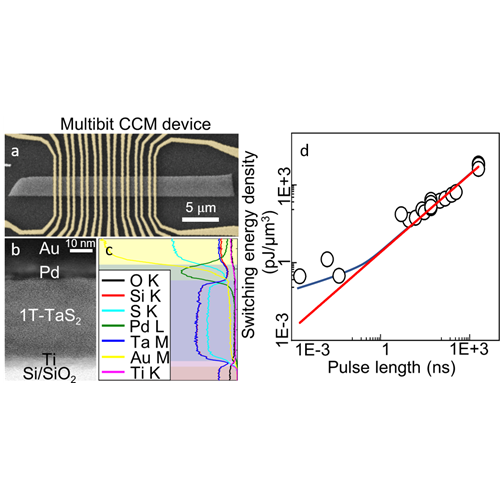
a) Multibit CCM device. b) TEM image of a cross-section. c) EDS analysis of the cross-section. d) CCM scaling law.
“We’ve shown that CCM devices can operate extremely well when measuring one memory element at a time. Now it’s time to scale up the design and produce a working memory array as it would be used in an actual computer system.” – Anze Mraz, Department for Complex Matter, Jozef Stefan Institute
CCM devices in the study demonstrate ultrafast switching speed (<16 ps), very low switching energy (2.2 fJ/bit), very good endurance (>107), non-volatility and a scalable design. Observed scaling law suggests that by reducing the dimensions of the device even further, the CCM devices could potentially be triggered by extremely small single flux quantum (SFQ) pulses used in superconducting SFQ logic circuits.
“Although this NFFA project had very challenging goals and was borderline feasible, it was of great scientific interest. Through a fruitful collaboration with the scientists from Slovenia, we managed to scale the CCM device down to the nanoscale, using state-of-the-art electron beam lithography.” – Dimitris Kazazis, Laboratory for X-ray Nanoscience and Technologies, Paul Scherrer Institute
Charge Configuration Memory Devices: Energy Efficiency and Switching Speed
Nano Lett. 2022, 22, 12, 4814–4821
NFFA Europe facilities that have been used to obtain the presented results are available at the Paul Scherrer Institut, Villigen, Switzerland.
Techniques used:
1) Vistec EBPG 5000PlusES e-beam lithography tool
2) Bruker Dimension Icon atomic force microscope

Dragan Mihailovic
Dragan Mihailovic is Head of Department for Complex Matter at the Jozef Stefan Institute, Director of the CENN Nanocenter, Professor of Physics at the University of Ljubljana and at the JS International Postgraduate School, where he is currently the Head of the Nanoscience program and Vice Dean. He leads a research group on nonequilibrium studies of quantum materials.
His two major current interests are mesoscopic metastable quantum states created through non-equilibrium processes using time-resolved methods in combination with scanning tunneling microscopy, and charge configuration topological memory devices.

Anze Mraz
Anze Mraz is a PhD student at the Department for Complex Matter at the Jozef Stefan Institute, Slovenia. His major current interest is the study of charge configuration topological memory devices.

